• Skip to main content
  • Skip to primary sidebar
  • Skip to footer

AggieFab Nanofabrication Facility

  • About
  • People
  • Equipment
  • Training
  • Fees
  • Become A User
  • Reservations
You are here: Home / Equipment / Semiprobe Probe Station & Keithley Paramter Analyzer

Semiprobe Probe Station & Keithley Paramter Analyzer

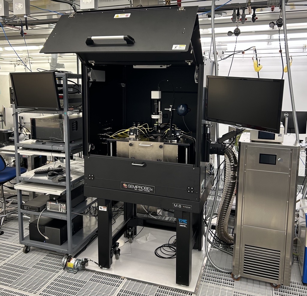
The Semiprobe PS4L Probe Station is a manual prober used for electrical characterization of wafer-level or chip-level devices. A Keithley 4200A SCS Parameter Analyzer is integrated with this probe station. This analyzer is highly accurate and versatile as it comes equipped with a Source Measure Unit (SMU), an ultrafast Pulse Measure Unit (PMU), and a Remote Preamplifier/Switch Module (RPM).

Probe Station Features:

Wafer Sizes: Up to 8″

Heating and Cooling: -60°C to 300°C

Isolation: Dark Box and Vibration Isolation Table

Parameter Analyzer Features:

OS: Windows 10

4211-SMU:

 – High power: Up to 21W, 1A range, and ±210V

 – High low current stability

 – Resolution down to 10aA w/ RPM

4225-PMU:

 – Measure range: ±40V and ±800mA

 – Minimum Pulse Width: 20ns

 – Simultaneous I & V Measurements

4225-RPM:

 – Enhanced resolution for PMU and SMU

 – Allows automatic switching between PMU and SMU


Probe Station SOP

Probe Station Flyer

See Current Trainer List for trainer to contact.

Primary Sidebar

Lithography/Patterning

Nanoscribe Photonics GT2 high-resolution 3D Printer Direct Laser Write Lithography

CEE X-Pro II Auto-Developer Workstation

UpNano NanoOne 1000 US 2PP 3D printer

Heidelberg MLA150 Maskless Lithography System

EVG 610 Double-sided Mask Aligner

CEE X-Pro II Spin Coater

Laurell Spin Coater

FEI Helios NanoLab 460F1 DualBeam Focused Ion Beam (FIB)

TESCAN MIRA3 E-beam Writer

Characterization

Woollam Alpha-SE Spectroscopic Ellipsometer

Bruker DektakPRO Profiler

Bruker Dimension Icon AFM

Evident LEXT Scanning Microscope​

Bruker FilmTek 2000

Semiprobe Probe Station & Keithley Paramter Analyzer

4 Dimensions 4 Point Probe

Caltex 3D Microscope

Nikon Eclipse LV150N Optical Microscope

Bonding/Dicing

MPP Wire Bonder

Disco Hi-Tec Dicing Saw

EVG 501 Wafer Bonder

Wet Processing

G&P POLI-400L Chemical Mechanical Polisher

G&N RC Plus Backside Grinder

Shellback Spin Rinse Dryer 820

Deposition/Diffusion

Cressington Gold Sputter Coater

Technic Semcon 1000 Cu Electroplater

Technic Semcon 1000 Ni Electroplater

CN1 Atomic Premium PEALD

CN1 Atomic Premium Thermal ALD

MTI RTP Anneal Furnace

Allwin21 AccuThermo AW610M RTP

Tystar LPCVD

Lesker PVD 75 E-Beam Evaporator 1

Lesker PVD 75 E-Beam Evaporator 2

Oxford Plasmalab 80 PECVD

Lesker PVD 200 DC Sputter

Lesker PVD 200 RF + DC Sputter

Minibrutes Oxidation/Anneal Furnace

PDS 2010 Labcoter2 Parylene Deposition System

Evatec CLN200E ScAlN Sputtering System 

Plasma Etching

Nordson March CS 1701 RIE tool

Plasma-Therm Corial F-Based ICP RIE

Oxford Estrelas DRIE

Samco UV-1 UV-Ozone Cleaner

Diener Plasma Cleaner

SPTS Xactix e2 XeF2 Etching System

Rapid Prototyping

PLS6.120D Laser Engraver

Roland MDX-50 Benchtop CNC

EnvisionTech 3D Printers

Other Equipment

Fume Hoods

Footer

AggieFab Nanofabrication Facility (AggieFab)

Frederick E. Giesecke Engineering Research Building
1617 Research Parkway
College Station, TX 77843

Texas A&M Engineering Experiment Station
Texas A&M University Department of Electrical and Computer Engineering
  • Accessibility
  • State Links and Policies
  • Privacy Notice
  • Website Feedback
  • Texas A&M University

Copyright © 2026 · Texas A&M Engineering Experiment Station · All Rights Reserved