• Skip to main content
  • Skip to primary sidebar
  • Skip to footer

AggieFab Nanofabrication Facility

  • About
  • People
  • Equipment
  • Training
  • Fees
  • Become A User
  • Reservations
You are here: Home / Equipment / TESCAN MIRA 3 for Electron Beam Lithography

TESCAN MIRA 3 for Electron Beam Lithography

TESCAN MIRA 3 for Electron Beam Lithography

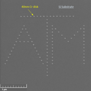
The TESCAN MIRA3 is a FE-SEM equipped with electrostatic blanker and DrawBeam software in order to write features on photoresist with dimensions of a few tens of nanometers.

Wafer Size: up to 20×20 mm

Source: Schottky Field Emission Gun

Acceleration voltage: 0.2-30 kV

Minimum electron beam spot size: ~ 2.5 nm

Minimum Electron beam current: ~10 pA

Import formats: GDSII and CAD

**Note** that AggieFab provides the following resists for use in the Tescan for ebeam lithography: S950 PMMA A4 and 494 PMMA A4.

Data sheet for PMMA resists

Data sheet for HSQ resists

AggieFab provides the following developers and strippers:

TMAH 25% in water
AZ 400T stripper
AZ developer 1:1
AZ 300 MIF developer
AZ 726 MIF developer
MIBK/IPA developer
MIF-319 developer

AggieFab also provides DisCharge EBL anti-charging agent:

DisCharge flyer

DisCharge data package

Please use the iLab system to schedule time to use this equipment.

TESCAN MIRA 3 Electron Beam Lithography sample image.

TESCAN MIRA 3 EBL Standard Operating Procedure

Primary Sidebar

Lithography/Patterning

Nanoscribe Photonics GT2 high-resolution 3D Printer Direct Laser Write Lithography

Suss MA-6 Mask Aligner

EVG 610 Double-sided Mask Aligner

BIDTEC SP100 Spin Coater

FEI Helios NanoLab 460F1 DualBeam Focused Ion Beam (FIB)

TESCAN MIRA3 E-beam Writer

Zeiss Orion Plus 5015 Helium Ion Microscope/NanoFab

Characterization

Veeco NT 9100 Profiler

Bruker DektakXT Profiler

Ocean Optics Film Measurement

Micromanipulator 6100 Probe Station

Veeco 4 Point Probe

Leica Reichert Polylite 88 Optical Microscope

Caltex 3D Microscope

Nikon Eclipse LV150N Optical Microscope

Bonding/Dicing

K&S Wire Bonder

Micro Automation Dicing Saw

EVG 501 Wafer Bonder

Deposition/Diffusion

Cressington Gold Sputter Coater

MTI RTP Anneal Furnace

Tystar LPCVD

ASM P8200/P3000 ALD

Lesker PVD 75 E-Beam Evaporator 1

Lesker PVD 75 E-Beam Evaporator 2

Oxford Plasmalab 80 PECVD

Lesker PVD 75 DC Sputter

Lesker PVD 75 RF Sputter

Minibrutes Oxidation/Anneal Furnace

PDS 2010 Labcoter2 Parylene Deposition System

CLUSTEX 100sp Sputter

Plasma Etching

Tegal Asher

Nordson March CS 1701 RIE tool

Oxford Plasmalab 100 ICP RIE

Rapid Prototyping

PLS6.120D Laser Engraver

Roland MDX-50 Benchtop CNC

EnvisionTech 3D Printers

Other Equipment

Laurell Spin Coater

Baxter Drying Ovens

Hot Plate Vacuum Chamber

Fume Hoods

Footer

AggieFab Nanofabrication Facility (AggieFab)

Frederick E. Giesecke Engineering Research Building
1617 Research Parkway
College Station, TX 77843

Texas A&M Engineering Experiment Station
Texas A&M University Department of Electrical and Computer Engineering
  • Accessibility
  • State Links and Policies
  • Privacy Notice
  • Website Feedback
  • Texas A&M University

Copyright © 2023 · Texas A&M Engineering Experiment Station · All Rights Reserved