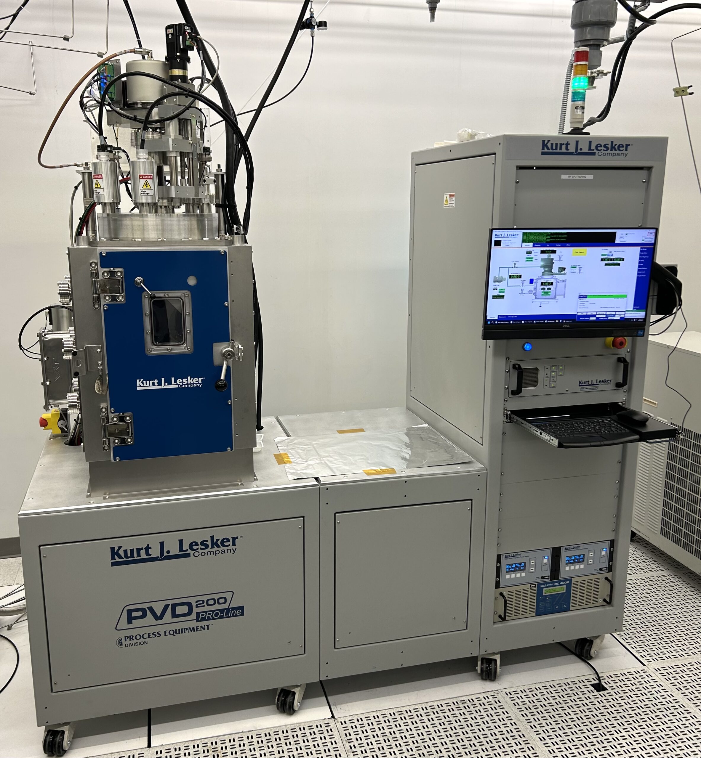
The LESKER PVD 200 RF Sputtering tool uses the RF sputtering technique to deposit thin layers of insulating materials. There are two RF sources allowing for co-sputtering, as well as one DC source which allows for deposition of conductive materials along with insulating materials without breaking vacuum.
- AggieFab provided target material: SiO2
- Target materials available for a nominal fee: Al2O3, AlN, and TiN
- Deposition orientation: Sputter Up
- Substrate size: up to 200 mm
- Substrate rotation: up to 20 rpm
Other materials can also be deposited in the RF sputter tool. Please review the list of approved materials to see if the material of interest is already allowed into AggieFab. If it is not, please forward the request for a new material to Sandra Malhotra ([email protected]), who will forward the request to the Material Review Board (MRB).

